Advanced PCB Design Techniques Using Sequential Build UpAuthor : Adrian September 11,solder paste specification 2025Table of ContentsIn the ever-evolving world of electronics, creating compact, efficient, and high-performing printed circuit boards (PCBs) is more critical than ever. For engineers and designers seeking advanced PCB design techniques, sequential build-up (SBU) offers a powerful solution to achieve high-density interconnects and optimized layouts. This blog dives deep into how sequential build-up routing, along with methods like via-in-pad and strategic component placement, can elevate your PCB designs to meet modern demands. Whether you're working on consumer gadgets or industrial systems, mastering these techniques can significantly improve signal integrity and space efficiency. Let’s explore the ins and outs of advanced PCB design with a focus on sequential build-up, breaking down its benefits, processes, and best practices to help you design better boards.
What Is Sequential Build-Up in PCB Design?Sequential build-up, often abbreviated as SBU, is a manufacturing and design technique used to create multilayer PCBs with high-density interconnects (HDI). Unlike traditional multilayer boards where all layers are laminated at once, SBU involves adding layers one at a time, allowing for precise control over via placement and routing. This method is particularly useful for advanced PCB design, as it enables the integration of microvias, blind vias, and buried vias, which are essential for compact and complex layouts. The primary goal of SBU is to increase the routing density while minimizing the board’s footprint. By stacking layers sequentially, designers can achieve finer line widths, smaller spacing, and better signal performance. This technique is widely used in smartphones, wearables, and other devices where space is at a premium. Why Choose Sequential Build-Up for Advanced PCB Design?Sequential build-up offers several advantages over conventional PCB manufacturing methods, making it a go-to choice for high-density interconnect projects. Here are some key benefits:
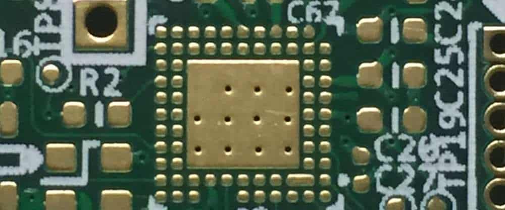
Key Techniques in Advanced PCB Design with Sequential Build-UpSequential build-up is just the foundation. To fully leverage its potential, designers must integrate other advanced techniques like high-density interconnect routing, via-in-pad, and strategic component placement. Let’s break down each of these elements and see how they work together in SBU designs. 1. High-Density Interconnect (HDI) RoutingHigh-density interconnect, or HDI, is a core component of advanced PCB design. It involves using fine lines (often less than 75 micrometers) and small vias (diameters as small as 100 micrometers) to pack more circuitry into a limited space. When combined with sequential build-up, HDI routing becomes even more effective, as each layer can be optimized for specific signals or power distribution. In practice, HDI routing with SBU allows designers to stack microvias directly on top of each other, known as "via stacking." This reduces the board’s overall thickness and improves electrical performance by shortening signal paths. For example, in a high-speed design operating at 5 GHz, shorter via lengths can reduce signal delay by up to 20%, ensuring better data transmission. Best Practice:Always plan your HDI routing before starting the SBU process. Use simulation tools to verify impedance matching and avoid signal reflections, especially for critical nets. 2. Via-in-Pad Technology for Space EfficiencyVia-in-pad is another game-changing technique in advanced PCB design. Traditionally, vias are placed away from component pads to avoid manufacturing issues. However, via-in-pad places the via directly within the pad of a surface-mount component, freeing up valuable board space for additional traces or components. In sequential build-up designs, via-in-pad is often used with microvias to connect layers without consuming extra real estate. This is particularly useful for ball grid array (BGA) components with fine pitch (e.g., 0.5 mm or less), where traditional via placement would be impossible. While via-in-pad can increase manufacturing complexity due to the need for via filling and planarization, the space savings—often up to 30% more routing area—make it worthwhile for HDI boards.
3. Strategic Component Placement for Optimal PerformanceComponent placement plays a vital role in the success of any PCB design, especially when using sequential build-up. Poor placement can lead to longer trace lengths, increased noise, and thermal issues, negating the benefits of HDI and SBU. In advanced PCB design, components must be arranged to minimize signal interference and optimize power delivery. For instance, place high-speed components closer to their corresponding connectors to reduce trace lengths, which can lower signal propagation delays to under 100 picoseconds per inch. Similarly, group power-hungry components near decoupling capacitors to stabilize voltage levels, often targeting a ripple of less than 50 mV. With SBU, you can also segregate sensitive analog and noisy digital circuits across different layers, reducing crosstalk by as much as 40%. Best Practice:Use a systematic approach to component placement. Start with critical components like processors and connectors, then position supporting elements like capacitors and resistors. Always consider thermal dissipation and layer-specific routing during placement.
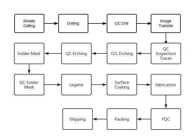
The Sequential Build-Up Process: Step by StepUnderstanding the sequential build-up process is essential for designers looking to implement advanced PCB design techniques. While the exact steps may vary based on the project, here’s a general overview of how SBU works:
The SBU process allows for incredible precision, but it requires careful planning to avoid issues like layer misalignment or via defects. Always collaborate with your manufacturing team to ensure design rules align with their capabilities.
Challenges in Sequential Build-Up and How to Overcome ThemWhile sequential build-up offers many benefits for advanced PCB design, it also comes with unique challenges. Being aware of these issues and knowing how to address them can save time and resources during the design phase. 1. Manufacturing ComplexityEach additional layer in SBU increases the risk of defects like via misalignment or delamination. To mitigate this, use design for manufacturability (DFM) guidelines and maintain tight tolerances, such as keeping via aspect ratios below 0.75:1 for reliable plating. 2. Cost ConsiderationsSequential build-up is often more expensive than standard multilayer fabrication due to the iterative process and specialized materials. To manage costs, limit the number of build-up layers to only what’s necessary and optimize your design for fewer via types. 3. Thermal ManagementHigh-density designs with SBU can generate significant heat, especially in compact boards. Incorporate thermal vias and heat sinks early in the design phase, targeting a thermal resistance of less than 1°C/W for critical areas.
Best Practices for Sequential Build-Up Routing in HDI DesignsTo maximize the effectiveness of sequential build-up in advanced PCB design, follow these best practices for routing and layout:
Conclusion: Elevate Your Designs with Sequential Build-UpAdvanced PCB design techniques like sequential build-up are transforming the way engineers create high-performance, compact circuit boards. By integrating SBU with high-density interconnect routing, via-in-pad technology, and strategic component placement, you can achieve designs that meet the stringent demands of modern electronics. While the process comes with challenges like manufacturing complexity and cost, the benefits of improved signal integrity, space efficiency, and design flexibility make it a worthwhile investment. Whether you’re designing for consumer products or industrial applications, mastering sequential build-up can set your projects apart. Focus on precision, collaborate with your manufacturing partners, and leverage the power of HDI to bring your innovative ideas to life. With these techniques in your toolkit, the possibilities for advanced PCB design are endless. Share · · · · The Role of Flux in PCB Wave Soldering: Selection, Application, and Residue RemovalMarch 16, 2026PCB wave soldering flux types include rosin, water-soluble, and no-clean options with varying activity levels for oxide removal and solder flow. This guide covers selection criteria, spray foam drop-jet application methods, residue removal processes, and alternatives like nitrogen blanketing to boost joint reliability and yields for engineers. Article Achieving Uniform Solder Fillets in PCB Wave Soldering: Process ControlMarch 16, 2026Achieve uniform solder fillets in PCB wave soldering with process control strategies. Optimize flux, preheat, wave height, conveyor speed for consistent fillet shape, height, and wetting balance. Includes visual inspection tips and troubleshooting for reliable through-hole assemblies. Boost quality in production. Article Optimizing Conveyor Speed for Efficient PCB Wave SolderingMarch 16, 2026Learn PCB wave soldering conveyor speed calculation to manage dwell time, immersion depth, and throughput effectively. Electric engineers get practical steps, best practices, and troubleshooting tips for higher process efficiency and fewer defects in wave soldering operations. Article Understanding IPC Standards for PCB Surface Finishes: Ensuring Quality and ComplianceMarch 11, 2026Understand IPC standards IPC 4552 ENIG and IPC 4553 immersion silver for PCB surface finishes. Ensure compliance, enhance solderability, and prevent common defects to achieve reliable, high quality circuit boards. Article Miniaturization Challenges in PCB AssemblyMarch 11, 2026Navigate the complexities of high density interconnect PCB assembly and precise component placement. Learn to tackle miniaturization challenges, from tiny part handling to thermal stress, ensuring robust and reliable electronics. Article High Speed Routing Techniques: PCBMarch 11, 2026Master high speed routing in PCBs to ensure signal integrity and minimize electromagnetic interference. Learn essential techniques for robust designs, from controlled impedance to differential pair strategies. Prevent performance issues and achieve reliable electronics. ArticleGet Instant PCB |